
US-based photonic manufacturing
100% USA supply chain
Multi-material photonics, built in California.
NantOptiFab brings lithium niobate and silicon photonics together in one integrated fabrication platform for AI interconnects, space systems, and quantum applications.
- LN
- ELN™
- PPLN
- TFLN
- SiPh
- SiN
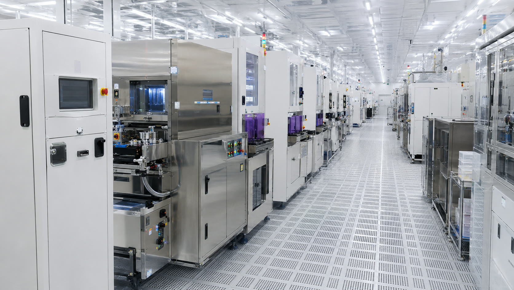
1,000+
precision tools across the fabrication flow
Active, passive, and nonlinear photonics
Design through precision packaging
AI, space, and quantum systems
Industry signals
Built around the work photonics teams are asking for.
An anonymized review of 122 recent industry conversations points to demand for technical partnerships, prototype access, process equipment, materials, packaging, validation, and specialized talent.
The material matters
No single platform does everything. Ours work together.
We match each optical function to the material that performs it best, then bring those functions together through vertically integrated process development, fabrication, and packaging.
01 / 06
Lithium Niobate
Proven electro-optic control with broad optical transparency
LN combines a strong electro-optic response, second-order optical nonlinearity, low optical loss, and high material stability.
- Core process
- Cleaning, Ti diffusion or proton exchange, electrode metallization, dielectric deposition, annealing
- Devices
- MIOC, IQ modulator, phase modulator, passive waveguide components
- Applications
- Fiber-optic gyroscopes, coherent LiDAR, space laser communication
02 / 06
Enhanced Lithium Niobate
Improved RF-to-optical interaction for faster devices
ELN™ uses wafer bonding and precision thinning to improve high-frequency response and optical field coupling while retaining the inherent optical strengths of lithium niobate.
- Core process
- Wafer preparation, surface treatment, bonding, thinning, metallization
- Devices
- Intensity and phase modulators, directional-coupler switches, coherent transmitters
- Applications
- High-speed modulation and ELN™-SiN heterogeneous photonic circuits
03 / 06
Periodically Poled Lithium Niobate
Engineered nonlinear interaction for quantum light and wavelength conversion
Periodic domain inversion enables quasi-phase matching and efficient access to lithium niobate’s strong second-order nonlinearity.
- Core process
- Wafer preparation, patterning, high-voltage poling, ridge-waveguide formation
- Devices
- SHG, optical parametric amplification, SPDC photon sources
- Applications
- Single-photon sources, squeezed-light generation, quantum communication
04 / 06
Thin-Film Lithium Niobate
High-speed modulation in a compact photonic footprint
TFLN pairs lithium niobate’s Pockels effect with tightly confined waveguides for fast, low-power optical systems.
- Core process
- Wafer preparation, patterning, waveguide etch, cladding, electrode metallization
- Devices
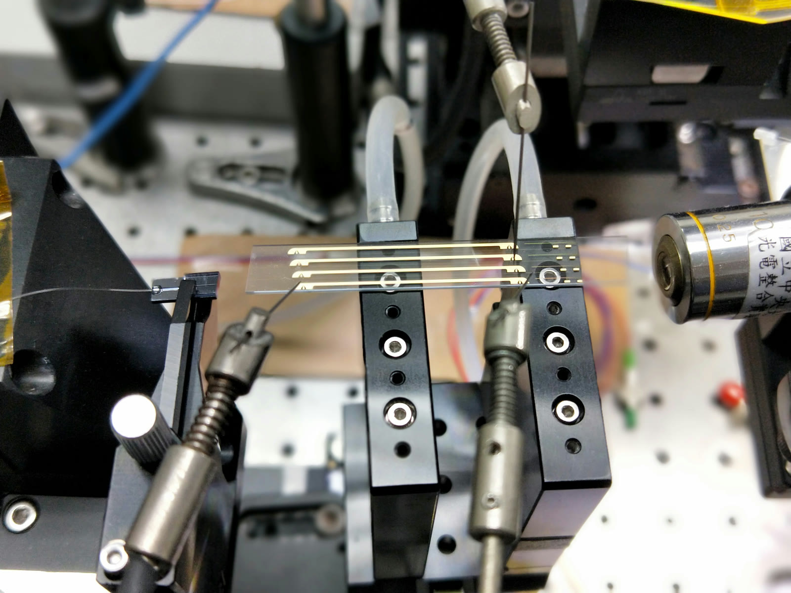
- Mach-Zehnder and ring modulators, phase shifters, couplers, spot-size converters
- Applications
- Coherent communication, optical switching, AI optical I/O, quantum processors
05 / 06
Silicon Photonics
CMOS-compatible density for complex optical engines
SiPh integrates optical routing, modulation, detection, and wavelength management on compact semiconductor-compatible circuits.
- Core process
- Waveguide fabrication, doping, Ge epitaxy, dielectric deposition, routing, passivation, wafer test
- Devices
- Coherent transmitters, DWDM transceivers, Ge photodetectors, optical engines
- Applications
- High-speed datacom, dense optical I/O, co-packaged optics
06 / 06
Silicon Nitride
Ultra-low-loss passive routing for integrated systems
SiN delivers low propagation loss, high-power handling, and scalable passive optical functions for photonic integration.
- Core process
- SiN deposition, waveguide patterning, cladding, metal routing, TSV and RDL formation
- Devices
- Photonic interposers, delay lines, edge couplers, wavelength filters
- Applications
- Co-packaged optics, quantum interference, heterogeneous integration
Heterogeneous integration
Put every photon on the right path.
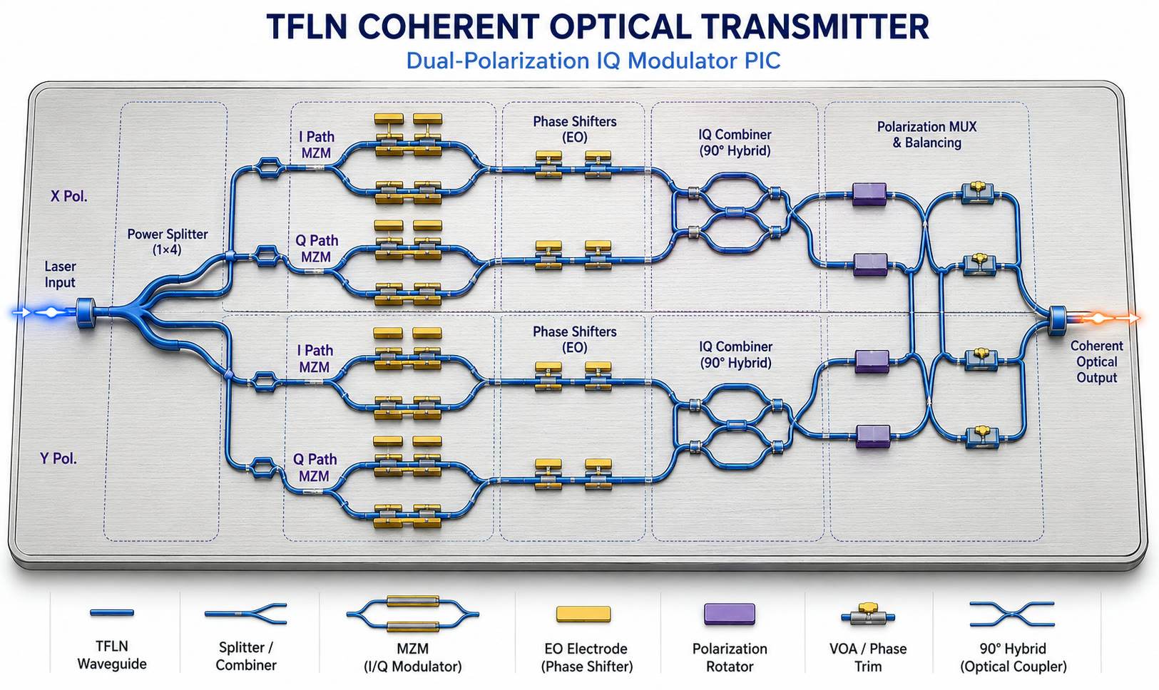
Combine active modulation, dense optical functions, nonlinear generation, and low-loss routing in increasingly integrated device architectures.
Active electro-optics
Passive routing
Nonlinear conversion
One roof. Full flow.
From material to tested module
A vertically integrated workflow connects device intent to repeatable wafer processes and precision photonic packaging.
- 01Design & simulation
Numerical analysis and device architecture
- 02Wafer fabrication
Lithography, deposition, etch, implant, and poling
- 03Dicing & faceting
Laser dicing, edge polishing, and facet preparation
- 04Photonic packaging
Fiber coupling, bonding, integration, and housing
- 05Test & quality
Optical and electrical probe, metrology, and QA
Thin-film deposition
PVD, CVD, LPCVD, sputter, and multi-material films
Photolithography
Coat, expose, develop, high-precision alignment, and e-beam patterning
Etch & strip
Dry and wet etch, selective pattern transfer, ashing, and residue removal
Thermal processing
Oxidation, diffusion, annealing, rapid thermal processing, and vacuum cure
Bonding & packaging
Wafer-level integration, die attach, fiber coupling, and wire bonding
Metrology & support
SEM, FIB, profilometry, optical inspection, clean, and implant
Selected toolmakers include AMAT, Axcelis, Canon, Evatec, KLA, Lam Research, Nikon, Oxford Instruments, Plasma-Therm, and SUSS MicroTec.
Application frontiers
Photonics for the systems that cannot stand still
Material-level control becomes system-level advantage where bandwidth, precision, power, and integration define the limit.
01
AI interconnects
Optical connectivity, closer to compute
TFLN, SiPh, and SiN support the shift from scale-out networks toward higher-bandwidth scale-up fabrics and scale-in optical I/O.
- High-speed electro-optic modulation
- Dense Tx/Rx integration
- Low-loss wavelength routing

02
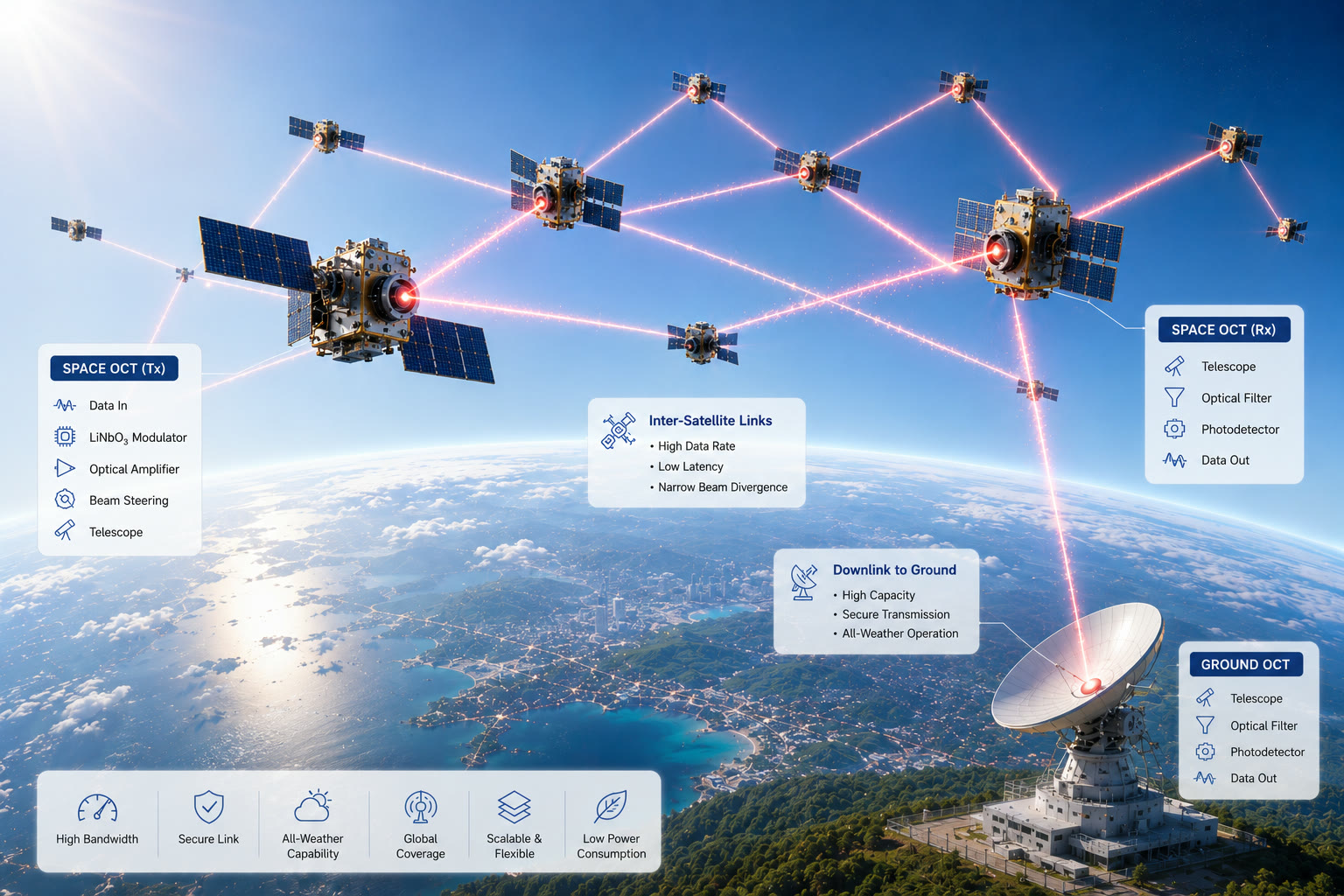
Space systems
Navigation, communication, and coherent sensing
LN, ELN™, and TFLN provide precise optical control for fiber-optic gyroscopes, optical communication terminals, and LiDAR.
- Stable rotation sensing
- High-capacity laser links
- Fast frequency and phase control
03
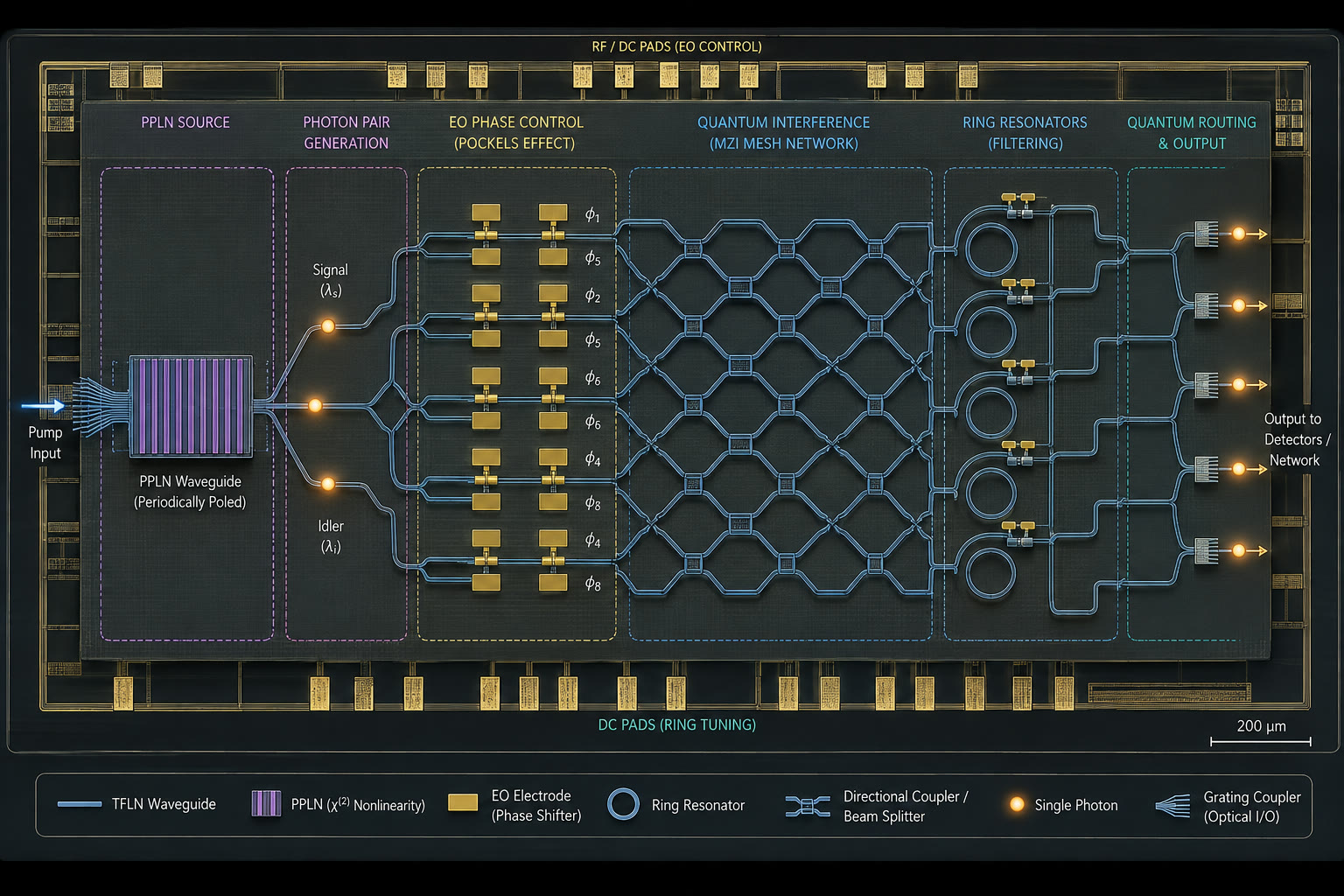
Quantum photonics
Generate, route, control, and detect quantum light
PPLN sources, TFLN and ELN™ control, and low-loss SiN circuits provide building blocks for QKD and photonic quantum computing.
- SPDC photon generation
- Adaptive phase control
- Low-loss interference and routing
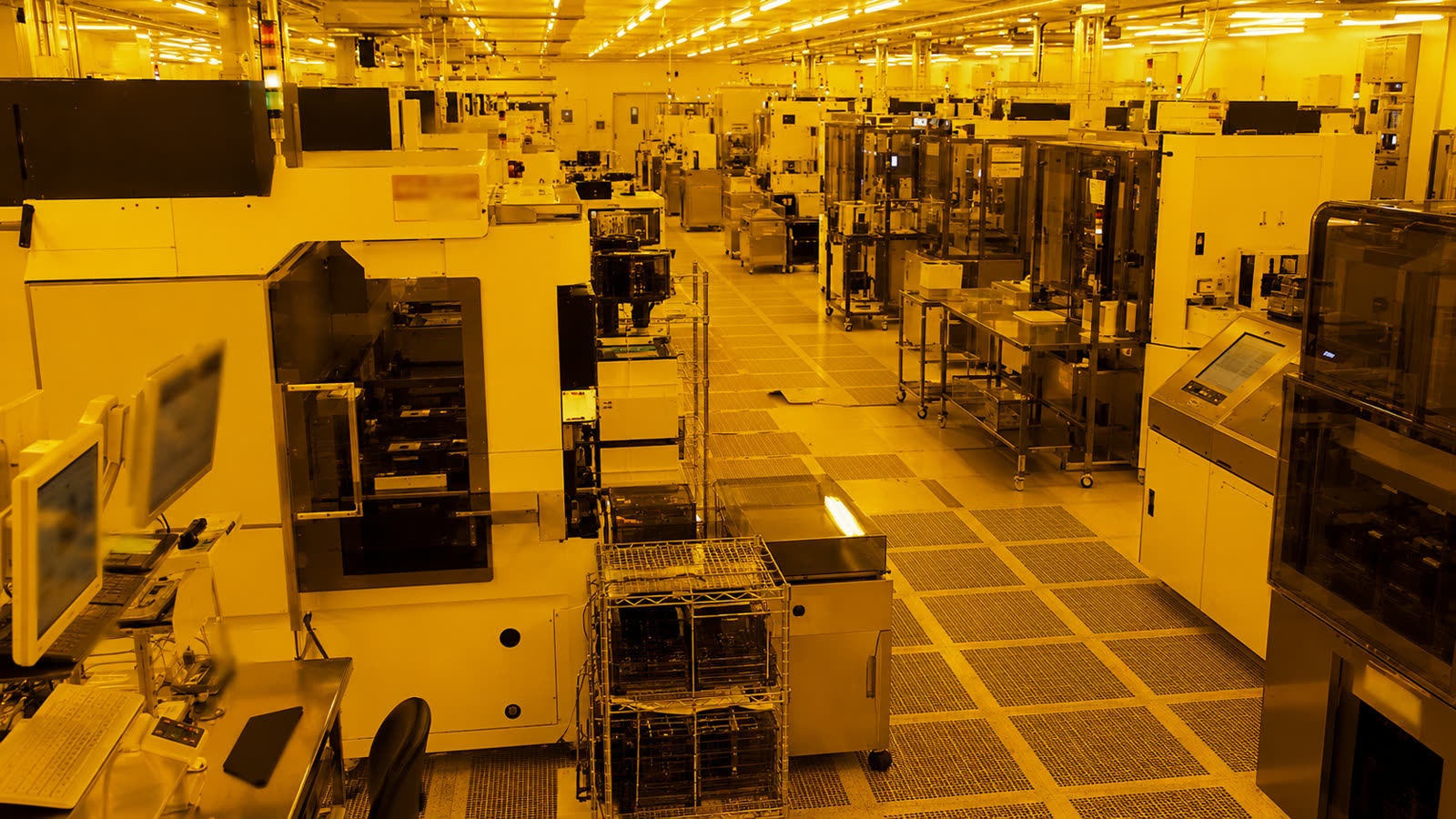
California fabrication
Built for precision. Set up for scale.
NantOptiFab’s California facilities bring together more than 1,000 precision tools across advanced patterning, film formation, material processing, packaging, and metrology.

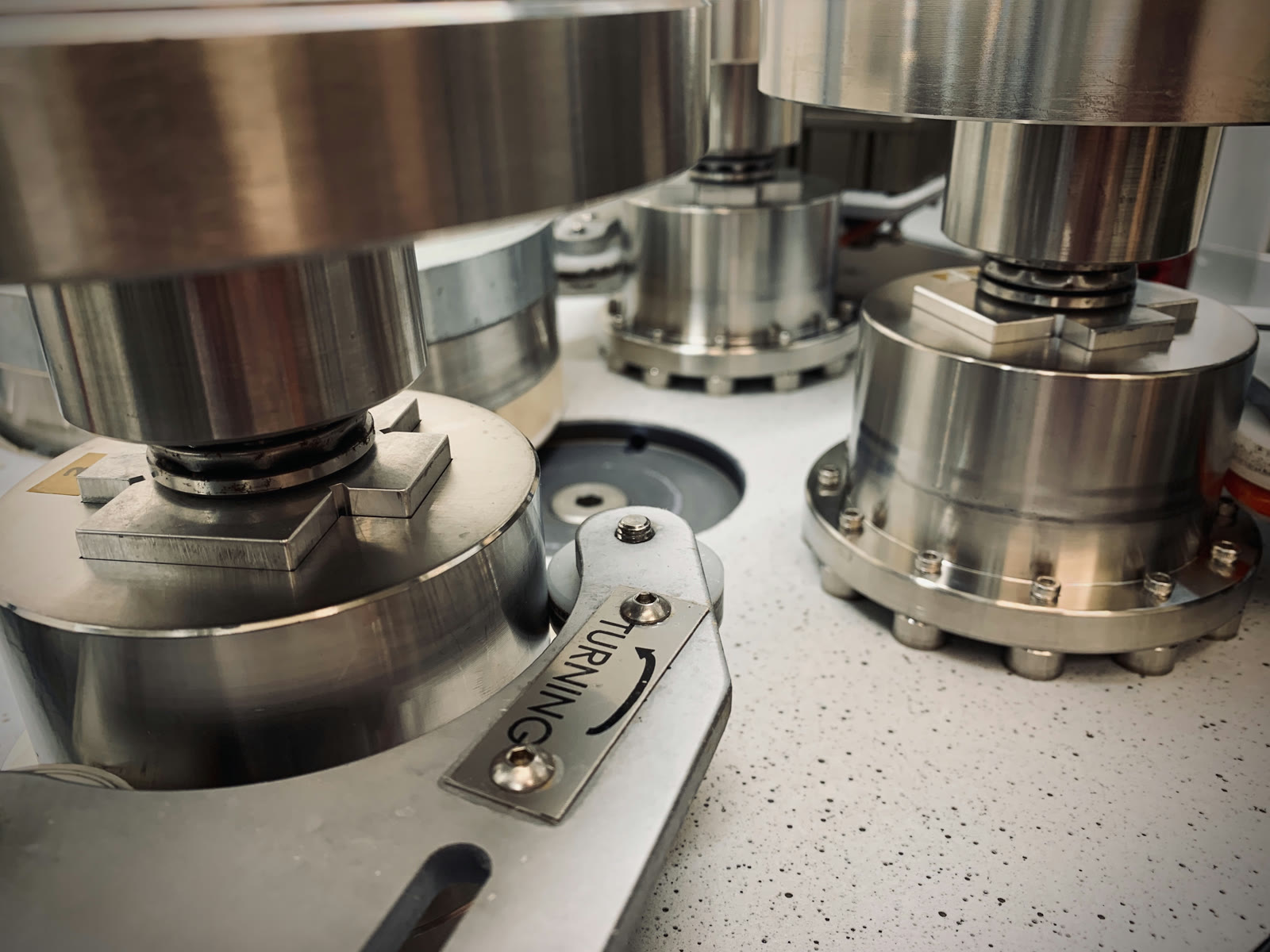
Load & transferRecipe-driven processIntegrated inspectionStable output
Start with the optical function
What are you building?
Tell our team about your target device, material platform, or integration challenge.
Start a conversationOr email us directly at info@nantoptifab.com
California, USA / www.nantoptifab.com