Company perspectives on American photonic manufacturing, complementary material platforms, vertical integration, and the systems driving the next generation of optical technology.
Market signals
What 122 industry conversations reveal
An anonymized analysis of recent industry engagement highlights near-term demand for technical collaboration, process equipment, materials, prototype access, integration, and talent.
Technical partners represented the largest audience segment at 47.5%, followed by suppliers and equipment providers at 27.9%. The strongest recurring technical themes included CPO and optical-module manufacturing, TFLN and silicon-photonics prototypes, advanced packaging, heterogeneous integration, and validation.
NantOptiFab unveils an American photonics roadmap for AI, space, and quantum
California-based NantOptiFab is advancing a six-platform technology roadmap for next-generation AI interconnects, space laser links, sensing, quantum communication, and photonic quantum computing.
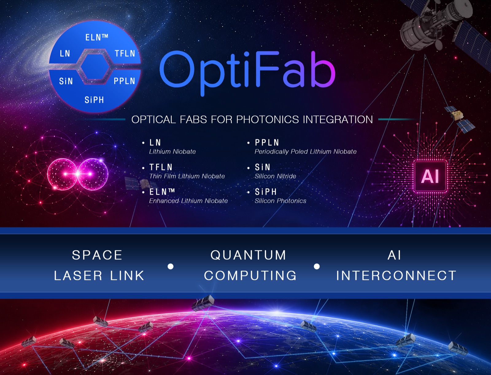
Built on four in-house optical wafer fabs with more than 107,600 square feet of fab space and monthly capacity exceeding 20,000 wafers, the company brings together LN, ELN™, PPLN, TFLN, silicon photonics, and silicon nitride. These complementary platforms cover high-speed electro-optic modulation, nonlinear optics, low-loss routing, photon detection, and dense photonic integration.
Three strategic application areas
AI interconnects: TFLN, SiPh, and SiN technologies for high-speed modulation, low-loss routing, integrated optical I/O, and next-generation compute infrastructure.
Space laser links: LN, ELN™, and TFLN technologies supporting navigation, high-speed optical communication, coherent sensing, and LiDAR.
Quantum photonics: PPLN, TFLN, ELN™, SiN, and detector technologies for quantum-light generation, optical control, routing, and integrated quantum systems.
NantOptiFab welcomes customers, technology partners, industry leaders, and strategic investors to explore collaboration in next-generation American photonics.
Multi-material platforms connecting space laser links, quantum computing, and AI interconnects.
Company strategy
Building a multi-platform integrated photonics strategy
NantOptiFab is building a technology and product brand focused on proprietary, multi-platform integrated photonics for American industry.
Six complementary platforms—LN, ELN™, PPLN, TFLN, SiPh, and SiN—support a progression from individual photonic functions toward increasingly integrated devices and circuits. Together they address electro-optic modulation, nonlinear processing, low-loss routing, optical detection, wavelength management, and dense integration.
Vertical integration as a technology foundation
Four in-house California optical wafer fabs connect materials, process development, device design, fabrication, dicing, faceting, packaging, and test. Closer interaction between materials, processes, and device development helps accelerate the validation of proprietary technology and product platforms.
Toward AI, space, and quantum
These markets share a growing need for higher performance, greater integration, lower loss, and more precise control of light. NantOptiFab connects its expertise in materials, processes, devices, and integration to create differentiated American technologies for each system frontier.
Long-term vision
The goal is a globally recognized American photonics technology and product brand—one that converts material-level expertise and proprietary intellectual property into manufacturable devices, integrated circuits, and complete system modules.
Technical perspective
Bringing TFLN and silicon photonics together for next-generation integration
As photonic systems move toward higher bandwidth, lower loss, and greater integration, no single material platform is optimized for every optical function.
Lithium niobate provides strong electro-optic response, low optical loss, broad transparency, and proven reliability. ELN™ enhances high-frequency electrical response and optical-field interaction. TFLN brings high-speed modulation into a compact integrated footprint. PPLN supplies quasi-phase-matched nonlinear conversion and quantum-light generation.
The strategy is to assign each optical function to the most suitable material, then combine electro-optic modulation, nonlinear processing, low-loss routing, detection, and dense integration in increasingly connected architectures.
This approach expands the design space for optimizing performance, optical loss, power, footprint, manufacturability, and integration at both the device and circuit level. From TFLN to silicon photonics, NantOptiFab is building a multi-material foundation for the next generation of integrated photonics.
Partner ecosystem
Connecting fabless PIC innovators and system integrators
NantOptiFab invites upstream designers and downstream integrators to shape the American photonics ecosystem together.
Engagement can begin with a material platform, device design, proprietary process, foundry flow, heterogeneous-integration challenge, package, or complete system-module objective. Exclusive ELN™ and TFLN patent and IP positions support the conversion of differentiated photonic ideas into heterogeneous integrated PICs.
Upstream
Design partners
Fabless PIC teams, universities, and device innovators seeking process-aware design and manufacturing access.
Core
Technology partners
Material, equipment, IP, and integration collaborators building differentiated platform capabilities.
Downstream
System integrators
AI, aerospace, communications, sensing, and quantum teams moving photonics into deployed products.