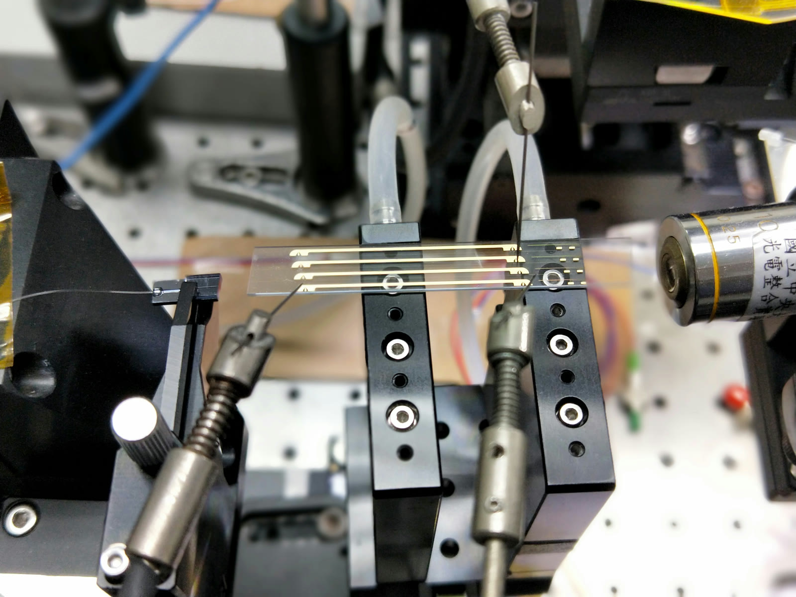
From numerical model to tested module.
Materials, process development, device design, wafer fabrication, dicing, faceting, photonic packaging, metrology, and quality assurance come together in one vertically integrated American workflow.
Design-to-module delivery
A connected workflow keeps material behavior, process constraints, device performance, package design, and verification aligned from the first simulation through final photonic test.
Design & simulation
Device architecture, numerical analysis, material selection, and process-aware simulation.
Wafer fabrication
Preparation, deposition, lithography, etch, implant, poling, metallization, and passivation.
Dicing & faceting
Laser dicing, wafer and chip singulation, edge polishing, and optical-facet preparation.
Photonic packaging
Fiber coupling, wafer and die bonding, wire bonding, housing, and module integration.
Test & quality
Optical and RF probing, photonic testing, metrology, inspection, and quality assurance.
Core fabrication toolset
The supplied capability inventory spans high-performance film formation, fine patterning, selective material removal, heterogeneous integration, thermal control, and analytical quality systems.
Physical vapor deposition
AJA International · AMAT · Evatec · MRC
Al, AlCu, Cu, Ti, Ta, Au, Ag, Cr, Ni, W, and Pt films for photonic devices and routing.
Chemical vapor deposition
AMAT · AMI · ASM · Evatec · Novellus
SiO₂, SiN, SiON, TEOS, USG, FSG, epitaxial Si/SiGe, CVD W, CVD TiN, and SAMs.
Coat and prepare
Cee / Brewer · FSI Polaris · TAZMO · TEL · SUSS
Photoresist, BCB, SOG, BARC, and HMDS primer coating for repeatable lithography.
High-resolution exposure
Canon · Elionix · Nikon · Raith · SUSS
Fine-pitch patterning, high-precision alignment, e-beam patterning, steppers, and nanoimprint lithography.
Photolithography development
FSI Polaris · Leatherwood · TEL · SUSS
Solvent and aqueous developer platforms supporting advanced photonic pattern definition.
Dry etch and pattern transfer
Lam Research · Oxford Instruments · Plasma-Therm
Oxide, nitride, poly-Si, and metal etch with anisotropic patterning, ICP-RIE, and IBE capability.
Selective wet processing
CFM · SEZ/EPCOS · SPEC · SVG
Wet chemical processing, selective SiO₂/SiN etch, and wafer-backside etching.
Strip and surface activation
GaSonics · Axcelis/Fusion · PVA TePla · Mattson
High-rate photoresist ashing, residue removal, and O₂/CF₄/H₂ surface activation.
Wafer-level integration
Applied Microengineering
Wafer bonding and 3D integration for ELN™, heterogeneous photonics, and multilayer devices.
Die and photonic packaging
Hesse & Knipps Bondjet 810 · ESEC 3018
Wire and wedge bonding for silicon-photonic and lithium-niobate devices, with fiber coupling and housing integration.
Diffusion and thermal processing
Bruce · BTU · Thermco · ASM · AMAT
High-temperature oxidation, dopant diffusion, LPCVD nitride/oxide, annealing, and poly-Si processing.
Rapid thermal and controlled bake
AG Associates · YES · Linn High Therm · Kendro
RTA 610/4100, HMDS vapor priming, vacuum curing, and controlled O₂/N₂ bake.
Analytical quality control
Bruker · Zeiss · NanoMetrics · Agilent · KLA
SEM, FIB, surface profiling, optical microscopy, AFM, GOI testing, loss metrology, and optical inspection.
Implantation and wafer cleaning
AMAT · Axcelis · DNS · Semitool
Ion implantation, wafer scrubbing, spin-rinse drying, wet benches, and process preparation.
Specialized photonic processes
Beyond the shared fab toolset, platform-specific modules support lithium-niobate waveguides, domain engineering, silicon detection, and low-loss heterogeneous systems.
| Module | Processes | Purpose |
|---|---|---|
| LN waveguide | Ti diffusion, proton exchange, annealing | Stable waveguides and electro-optic devices |
| PPLN poling | High-voltage poling, PFM verification, SHG characterization | Quasi-phase-matched nonlinear conversion |
| TFLN patterning | Fine lithography, waveguide etch, cladding, electrodes | Compact, high-bandwidth electro-optics |
| Silicon photonics | Doping, Ge epitaxy, routing, passivation, probe | Integrated modulation, detection, and optical I/O |
| SiN integration | Low-loss deposition, edge coupling, TSV and RDL | Passive routing, interposers, and quantum circuits |
| Backend | Laser dicing, facet polishing, electroplating, fiber attach | Optical interfaces and packaged modules |