
Four dedicated fabs. One connected system.
NantOptiFab designs, fabricates, packages, and tests photonic integrated circuits through specialized California facilities spanning lithium niobate, nonlinear photonics, silicon nitride, and silicon photonics.
Specialized around the material
Each fab concentrates the processes and equipment needed by its platform while sharing design, backend, packaging, metrology, and quality infrastructure across the full manufacturing system.
LN & TFLN Fab
3,000+wafers per month
High-speed electro-optic modulators, coherent devices, and ultra-broadband transceivers.
ELN™ & PPLN Fab
3,000+wafers per month
Enhanced electro-optics, wavelength converters, and quantum photon sources.
Silicon Nitride Fab
10,000+wafers per month
Ultra-low-loss devices, passive routing, and wafer-level photonic interposers.
Silicon Photonics Fab
5,000+wafers per month
800G/1.6T CPO modules, integrated Tx/Rx, and AI-interconnect PICs.
Combined production is communicated conservatively as 20,000+ wafers per month across the four dedicated California fabs.
White light and yellow light, connected
Wafer preparation, film formation, integration, backend, packaging, patterning, metallization, and PPLN domain engineering are arranged as one coordinated workflow.
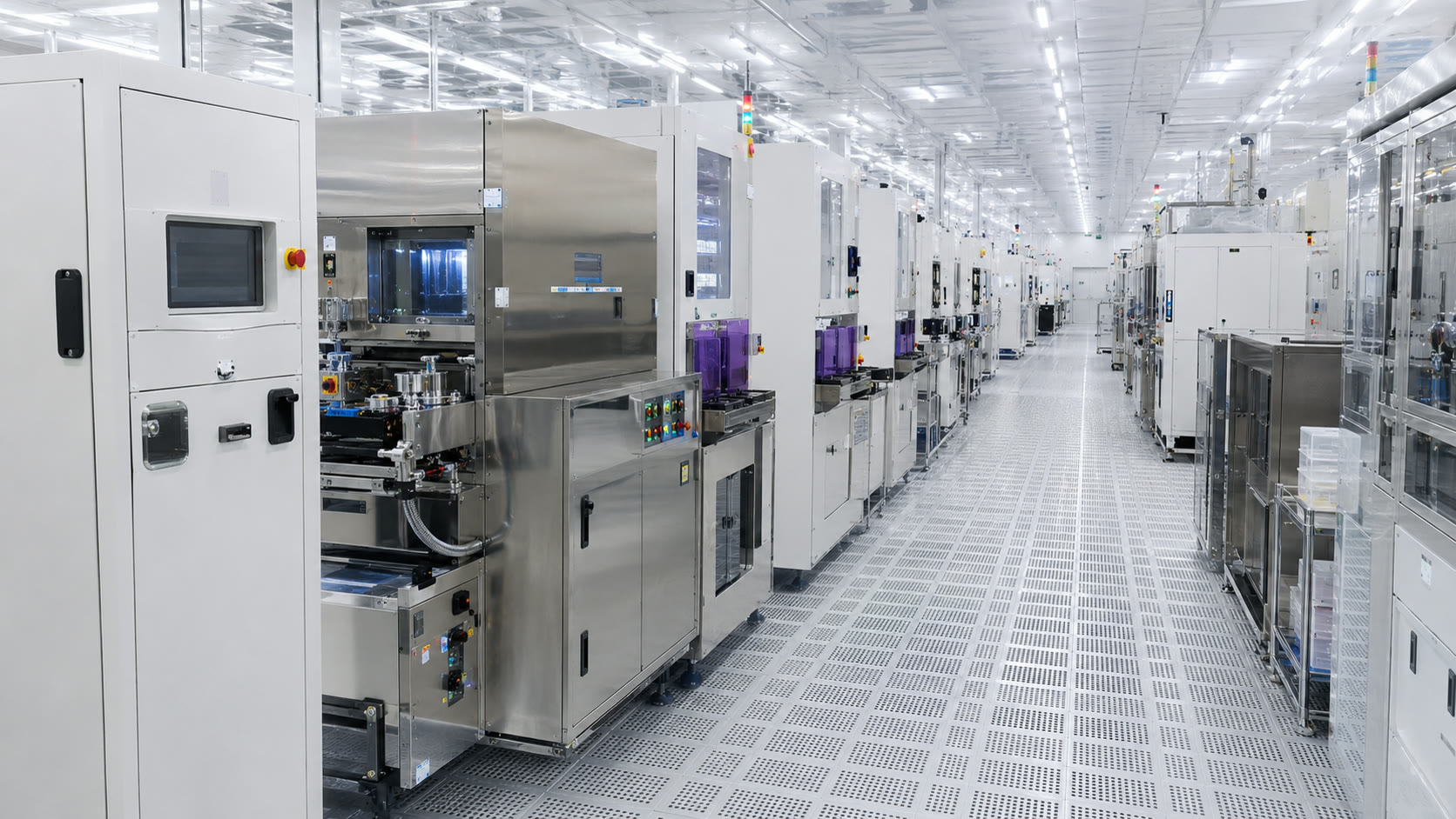
White light area
Wafer processing
Wafer preparation, PECVD, LPCVD, sputtering, bonding, CMP, implantation, integration, packaging, and metrology across six process modules.
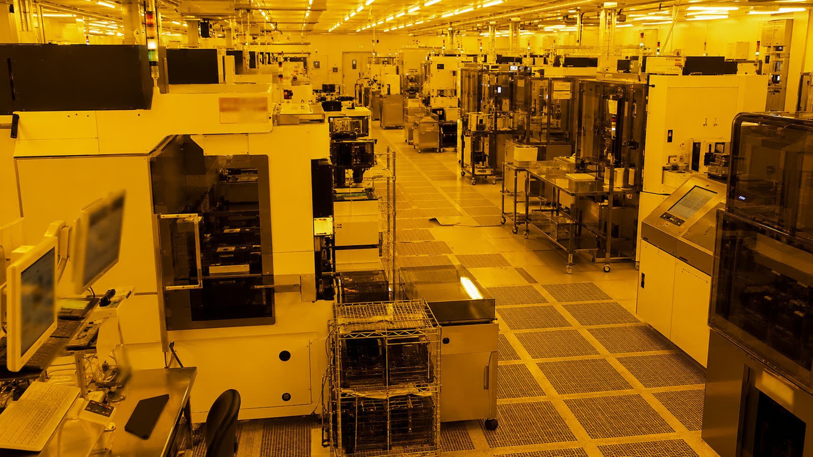
Yellow light area
Patterning & poling
Coating, exposure, development, stepper and e-beam patterning, ICP-RIE, IBE, lift-off, metallization, high-voltage poling, PFM, and SHG verification across five modules.
Automation in action
Automated equipment connects critical steps into one repeatable wafer workflow, increasing controlled throughput and process consistency across material platforms.
Load & transfer
Controlled wafer movement into the qualified process sequence.
Recipe-driven process
Automated execution using defined platform and device recipes.
Wafer inspection
Integrated optical and process verification at critical control points.
Stable output
Consistent execution, traceability, and repeatable manufacturing.
Quality assurance
Final metrology, optical test, electrical test, and delivery review.
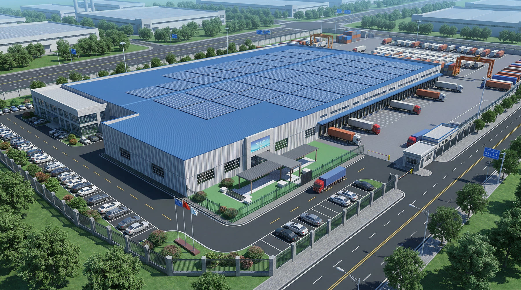
Built for repeatable scale
Dedicated platform capacity is paired with common analytical, packaging, and quality infrastructure so programs can move from development through repeatable production without changing partners.
| Production system | Platform role | Representative output | Monthly capacity |
|---|---|---|---|
| LN / TFLN | Electro-optic modulation | Modulators and broadband transceivers | 3,000+ |
| ELN™ / PPLN | Enhanced EO and nonlinear optics | Coherent devices and photon sources | 3,000+ |
| SiN | Ultra-low-loss passive photonics | Interposers, filters, and quantum circuits | 10,000+ |
| SiPh | Dense electronic–photonic integration | CPO modules and AI interconnect PICs | 5,000+ |
100% USA supply-chain positioning
The NantOptiFab program is presented as California-based, American photonic manufacturing. All geographic references, partnership language, and facility positioning across this site follow that operating model.
California foundation
Facility, engineering, manufacturing, packaging, and customer-facing language is centered on California and the United States.
Fewer handoffs
Materials, process development, device design, wafer fabrication, backend, packaging, and test are coordinated under one manufacturing organization.
Built for partners
Fabless PIC designers, system integrators, universities, and downstream product teams can engage at the stage that matches their program.